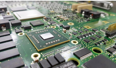
Before an electronic product can be tested in the real world, its digital PCB design needs to become a physical circuit board. This process begins with manufacturing files and ends with a bare PCB that engineers can inspect, test, and use as the foundation for further development.
For buyers, selecting the right fabrication partner is about more than finding the lowest price or fastest advertised delivery. Layer count, stack-up, impedance requirements, DFM support, line and spacing capabilities, and manufacturing lead time can all affect whether a prototype accurately represents the intended design.
Start With the Gerber and Drill Files
Bare-board PCB fabrication begins when the manufacturer receives the required production files.
Gerber files contain the artwork information needed for individual PCB layers, while drill files define the locations and dimensions of holes and vias. Depending on the design, the manufacturing package may also contain information about board thickness, copper weight, surface finish, dimensions, impedance requirements, and the intended layer stack-up.
The manufacturer should review these files before production begins. Missing information, incorrect file versions, or inconsistencies between different design outputs can cause manufacturing delays.
A careful initial review helps ensure that the fabricator is working from the correct design and understands the requirements of the prototype.
Use DFM Before Manufacturing
A PCB may be electrically correct while still containing features that are difficult to manufacture consistently. This is why Design for Manufacturing, or DFM, should be considered before the fabrication process starts.
DFM review can identify concerns involving trace width, spacing, drill sizes, vias, copper clearances, board edges, and other fabrication constraints. Resolving these issues before production can prevent avoidable prototype failures and reduce the chance of having to reorder the board.
DFM can also help engineers determine whether their chosen layer structure and physical design are practical for the selected manufacturing process.
For prototypes, this early engineering input is especially useful because the purpose of the first board is to provide meaningful test results, not simply to produce a physical copy of a computer file.
Choose the Correct Layer Count
Layer count has a major influence on PCB construction and routing.
Simple circuits may only require two layers, while more complicated designs may need four, six, eight, or twelve layers. Additional layers can provide more routing space and allow engineers to separate signal, power, and ground structures more effectively.
However, adding layers unnecessarily can increase manufacturing complexity and cost. Buyers should therefore select a layer count based on the electrical and mechanical requirements of the design.
FastTurnPCB provides defined prototype fabrication timelines according to layer count. Its stated lead times are approximately 48 hours for 2–4 layer boards, 3 days for 6–8 layer boards, and 5 days for 10–12 layer boards.
These timelines illustrate why layer count should be considered when planning a prototype schedule.
Build an Appropriate Stack-Up
The stack-up determines how the copper layers and insulating materials are arranged inside the PCB.
A suitable stack-up is important for both physical construction and electrical performance. The distance between signal layers and reference planes can affect controlled impedance, while the overall material arrangement influences board thickness and other characteristics.
For this reason, buyers should not simply tell a fabricator how many layers they need. The manufacturer should also understand the required stack-up and confirm that it can be manufactured according to the project’s specifications.
For prototypes intended to represent a future production board, using a suitable stack-up from the beginning can make later testing more meaningful.
Pay Attention to Impedance Control
High-speed electronic designs often have specific impedance requirements. Signal traces need to be manufactured with appropriate geometry and positioned relative to reference planes to achieve the intended electrical characteristics.
Impedance is influenced by several factors, including trace width, copper thickness, dielectric thickness, and material properties.
FastTurnPCB states an impedance tolerance of ±5% for its PCB manufacturing capabilities. Buyers with controlled-impedance requirements should provide their target values to the manufacturer before production and confirm that the proposed stack-up and fabrication process can support them.
This is another reason engineering communication should happen before fabrication rather than after the boards have already been produced.
Consider Line Width and Spacing
As PCB layouts become denser, trace width and spacing become increasingly important.
A fabricator needs to reproduce the copper geometry specified in the design without compromising manufacturing consistency. Very fine traces can require more advanced fabrication capabilities, particularly when combined with multiple layers and tightly packed routing.
FastTurnPCB supports 2.5/2.5 mil line width and spacing, which can accommodate demanding prototype designs that require fine routing.
Nevertheless, buyers should avoid using extremely small geometries unless the design actually requires them. More generous trace widths and spacing can provide greater manufacturing margin when the electrical requirements allow it.
Fast Fabrication Still Requires Controlled Manufacturing
Short fabrication lead times can be extremely valuable during product development. Engineers can receive physical boards sooner, perform testing, identify problems, and move more quickly toward the next revision.
However, speed should never mean skipping engineering review or manufacturing controls. prototype PCB fabrication should combine rapid production with DFM support, accurate layer construction, controlled impedance, suitable stack-up design, and reliable manufacturing processes.
A prototype delivered quickly but built incorrectly can create more delays than a properly manufactured board delivered a little later.
When comparing suppliers, buyers should therefore evaluate both how fast a manufacturer can produce the board and how consistently it can meet the design specifications.
Select Materials Carefully
The PCB material affects electrical, mechanical, and thermal performance. Standard FR-4 is suitable for many conventional applications, but some designs may have more specific material requirements.
Material selection should be considered together with the stack-up and impedance requirements. Changing the dielectric characteristics or board construction can affect controlled-impedance calculations and potentially influence the behavior of the prototype.
For this reason, the fabricator should confirm the proposed material system before production rather than making substitutions without engineering approval.
Review Drilling and Plating Requirements
Once the board structure and copper artwork have been established, drilling and plating become important parts of the manufacturing process.
Drilling creates through-holes and other required openings, while plating establishes conductive connections between appropriate copper structures. The accuracy of these processes contributes to the finished board’s electrical and mechanical performance.
Vias and plated holes should therefore be reviewed as part of the overall fabrication requirements. Designs with small holes, dense routing, or complex multilayer structures may require particular attention during manufacturing review.
A capable supplier should be able to confirm that the required drilling and plating specifications are compatible with its fabrication process.
Inspect the Finished Bare PCB
After fabrication, the finished prototype should be checked against the original design requirements.
Depending on the project, engineers may verify:
- Overall board dimensions
- Layer count and construction
- Trace width and spacing
- Hole and via locations
- Board thickness
- Copper requirements
- Surface finish
- Impedance specifications
- Cutouts and edge features
- General board workmanship
Defining these acceptance requirements before production makes it easier to evaluate whether the delivered prototype is suitable for testing.
Plan Lead Time Around Design Complexity
Prototype schedules should account for the complexity of the PCB rather than assuming every board can be manufactured within the same timeframe.
A two-layer or four-layer board may be produced much faster than a ten- or twelve-layer design. The additional layers require more manufacturing steps and greater control over registration and material construction.
FastTurnPCB’s stated timelines of 48 hours for 2–4 layers, 3 days for 6–8 layers, and 5 days for 10–12 layers provide a useful framework for planning prototype requirements.
Buyers should confirm the exact lead time for their board before placing an order, particularly when special materials, controlled impedance, or other manufacturing requirements are involved.
Make the Prototype Representative
A prototype is most useful when it accurately represents the intended product design.
Whenever possible, the prototype should use an appropriate layer count, stack-up, material structure, impedance configuration, and manufacturing approach. This helps ensure that electrical and mechanical testing produces information that can be applied to later revisions.
If the prototype is manufactured using a substantially different construction simply to reduce cost or production time, some test results may not accurately reflect the behavior of the intended final PCB.
Assembly Can Be the Next Step
Once the bare PCB has been successfully fabricated and inspected, the next stage may be component assembly.
Assembly is an optional continuation of the prototype workflow and can turn the finished bare board into a functional electronic prototype. However, the fabrication stage should first ensure that the PCB itself meets the required design and manufacturing specifications.
Keeping fabrication and assembly with one supplier can simplify logistics when both services are required, but buyers should evaluate the bare-board manufacturing capabilities separately.
Final Thoughts
Prototype PCB fabrication is the process that transforms a digital PCB design into a physical foundation for electronics testing. The quality of that process depends on much more than simply transferring Gerber artwork onto copper.
Layer count, stack-up, impedance, line and spacing requirements, materials, drilling, plating, DFM, and lead time all deserve attention before an order is placed. A capable manufacturer should be able to review the design, identify manufacturing concerns, and produce the bare PCB according to the project’s technical requirements.
Fast fabrication can accelerate development, but controlled manufacturing is what makes a prototype genuinely useful. By evaluating both engineering support and production capabilities, buyers can reduce avoidable revisions and obtain boards that provide meaningful results during the next stage of product development.
For manufacturers looking to support this process, FastTurnPCB offers prototype PCB fabrication with DFM support, 2.5/2.5 mil line and spacing capability, ±5% impedance tolerance, and stated prototype lead times based on PCB layer count.